

Tools We Support
Quaestor Q+
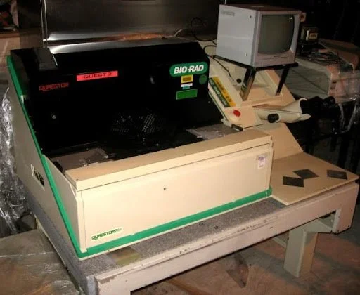
The early overlay and CD tool, which laid the groundwork for the advanced Q3-8 tool family, was designed for full automation using detailed recipes and advanced image-based measurements. Each Q+ system came with a high-quality Kensington stage and a custom wafer handling system that could manage wafers from 3 to 8 inches. This tool also served as an opti-station, enabling thorough defect analysis and precision in semiconductor manufacturing.
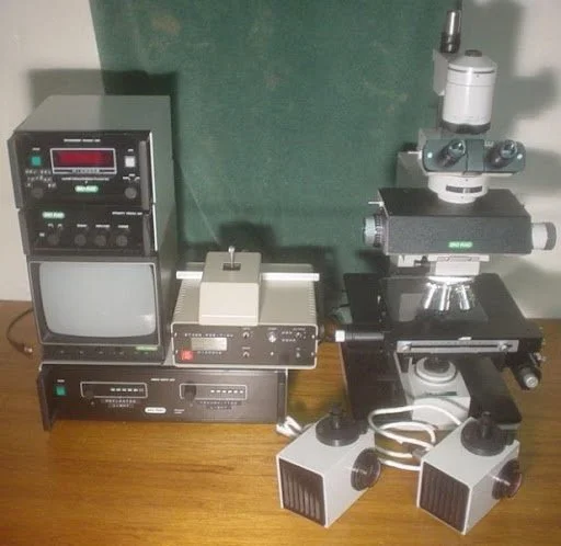

M41 Photoplan Series
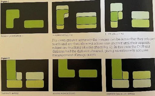
Vickers Instruments has created advanced measuring microscopes that include a special module to produce two identical images of a feature. By adjusting these images vertically and calibrating the movement, users can measure complex structures accurately. They can see where the two images touch, and once the process is done, the measurement appears on a clear screen. The system is fully manual, requiring users to place samples on a stage, align them, and perform a "shear" process. After this, they can easily read the measurement. The microscope offers two types of shear: single and double, allowing for flexible measurement options.
Optical metrology is a quick method to measure structures on semiconductor wafers, whether they are CD line / pitches or overlay / registration marks, the alternative method would be a SEM (scanned electron microscope) which is slow compared to optical methods. Typical magnifications for all tools made by Bio-Rad, Accent and Nanometrics is 4x (alignment) and 70x (measurement). Earlier tools had a turret with a 30x and 140x objectives, these were seldom used so the later models had fixed optics; this provided the best precision and lowest TIS (tool induced shift).
Q3-8 Metrology Tools
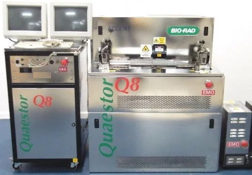
The advanced Quaestor tools manufactured by Bio-Rad and Accent have successfully led to the development of the Q3-8, which is a highly flexible system designed with upgradeable parts to enhance its functionality and longevity. This innovative system utilizes automated optical technology specifically for processing wafers ranging from 3 to 8 inches in size. Each individual system is equipped with a Kensington stage along with a custom wafer handler, both of which significantly contribute to high operational efficiency. Moreover, these advanced tools are capable of connecting to one another, allowing engineers to maintain consistent production recipes across different machines, ensuring reliability and quality in output. The light source utilized in this system is a broad band xenon, which is further enhanced by six customizable color filters that can be tailored to meet the specific needs of each individual customer.
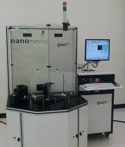
Q220/230/240 Metrology Tools
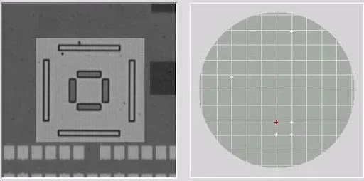
The Q2x0 series offers a comprehensive and upgradeable optical metrology suite, allowing customers to begin their experience with a more affordable tool and progressively enhance its capabilities as their production requirements evolve over time. As production demands continually increase for enhanced throughput, improved precision, and reduced Total Induced shift (TIS), the optics module can be easily replaced and modified to meet more complex performance criteria. Each Q2x0 tool operates seamlessly on a robust and reliable Linux operating system and is equipped with a high-performing Genmark robot and an Anorad stage, which features sophisticated XYZ and theta axes for precise alignment and measurement tasks. These advanced tools can be interconnected efficiently, enabling process engineers to ensure uniformity and consistency across an entire fleet by maintaining the same recipe revisions, facilitating streamlined operations. The light source utilized in the Q2x0 tools is a versatile broadband xenon lamp, which can be customized with either 6 or 8 color filters based on the specific and varying needs of customers. As users transition to later models, these systems primarily focus on accurately measuring overlay and registration targets. In typical operational scenarios, the outer mark consists of distinct bars printed during the previous layer, while the inner mark contains neatly arranged bars printed in the most recent layer, which are often structured as 25um squares. The core function of the metrology tool is to accurately assess and verify the critical alignment of the inner mark to the outer mark in both the X and Y directions, thereby ensuring precise calibration for efficient manufacturing processes.
IVS 120 - 185 (DOS)
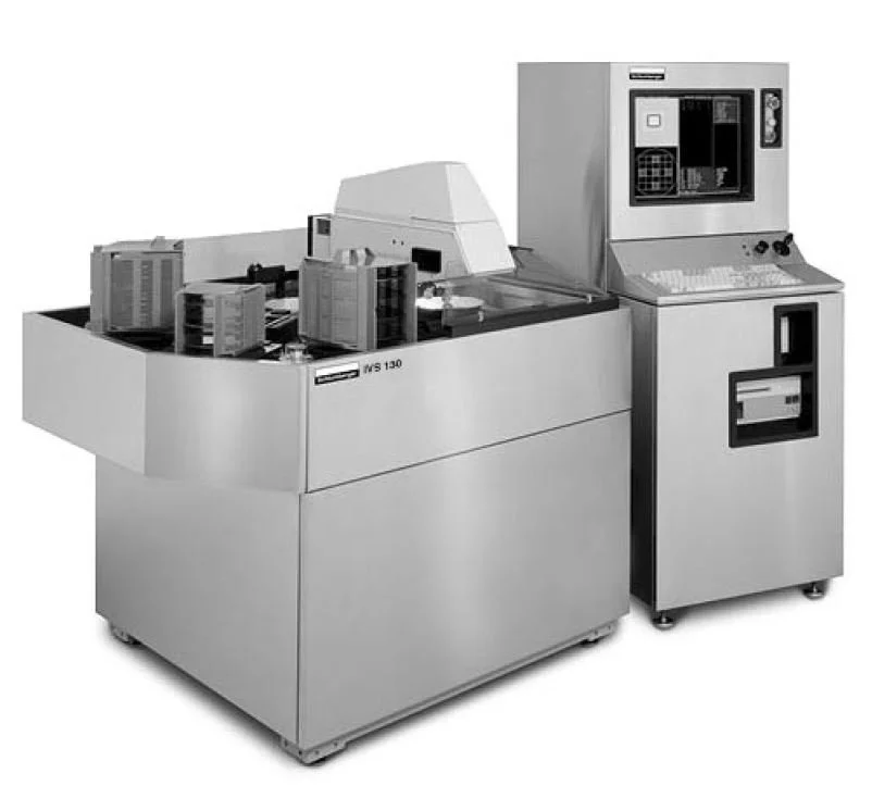

The IVS automatic metrology tool is designed for fast, precise, and unattended measurement of semiconductor, MEMS, LED or other wafer-based features. It provides accurate and precise measurement of overlay registration (RG) features and critical dimensions (CD’s) as well as Z (feature height) and other specialized measurements. IVS tools provide accuracy and repeatability for the most demanding applications.
The IVS brand has become known for reliable, repeatable automated metrology. A few of the features IVS-brand tools include the metrology automated process, Front Surface Focus, pattern recognition, and the advanced metrology algorithms contained in the system.
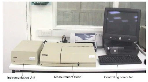
PN 4200/4300
Original profiler, bench mounted, tool includes measurement head, Instrumentation unit and PC. A PVS unit can be added and fits under the measurement head.
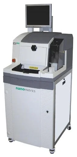
ECV PRO
Successor to the PN4300 profilers, a standalone tool including images of the etch pit, recipe based with 2 types of light sources
Electronic devices are engineered by selectively introducing impurities into substrate semiconductor materials or by depositing (growing) new layers epitaxially onto the surface of the bulk. The properties of the device are determined by the nature of the impurities and substrate and by the carrier concentration and spatial distribution of the various regions. The processes used to engineer these structures are often complex, and the results are highly dependent on purity of starting materials and the processing route. As device operation depends on the electrical activity of the species and not on their chemical concentration it is appropriate to evaluate the material by measurement of its electrical characteristics. Among the many parameters that can be measured, carrier concentration versus depth is one of the most useful and widely used.
The major techniques used for determining the 'electrical' carrier concentration as a function of depth are capacitance/voltage (C-V) measurements, spreading resistance, and differential hall. Spreading resistance involves a lot of time-consuming sample preparation and complex data processing, and the results are highly dependent on the skill of the operator. On the other hand C-V measurements employing a Schottky contact are relatively straightforward. The principal limitation is the depth of profiling which is constrained by the reverse breakdown voltage of the Schottky diode. This is a serious consideration in materials with high carrier concentrations where the depletion layer is very narrow.
The Electrochemical C-V Profiler (ECV) overcomes this limitation by employing an electrochemical etching system. By making use of a well-defined electrochemical dissolution reaction, the material can be profiled to any depth at a controlled and calculated rate. The semiconductor/electrolyte interface behaves as a Schottky diode and thus permits carrier concentration measurements to be made in the conventional manner.
By using an electrolyte to both etch and form a Schottky contact with the semiconductor, the ECV Profiler has become the most effective method of determining the efficiency and success of a process prior to device manufacture.